Semiconductor Wafer Inspection Equipment Market by Segments, Country and Region – Global Market Size Estimation, Industry-Wide Analysis, Competitive Landscape Assessment & Long-Term Forecast to 2032

8.22%
CAGR (2026-2032)
6.92 USD Bn.
Market Size
326
Report Pages
123
Market Tables

Overview

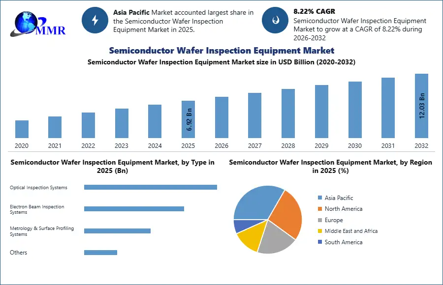
Semiconductor Wafer Inspection Equipment Market size was valued at USD 6.92 Bn in 2025 and the total Semiconductor Wafer Inspection Equipment revenue is expected to grow by 8.22% from 2026 to 2032, reaching nearly USD 12.03 Bn by 2032.

Semiconductor Wafer Inspection Equipment Market Overview

The semiconductor wafer inspection equipment is designed to detect small defects and accurately locate their coordinates automatically. These provide highly consistent and reliable outcomes. The Semiconductor Wafer Inspection Equipment market includes a wide range of equipment and technologies designed to ensure the integrity and performance of semiconductor wafers that are foundational to producing integrated circuits (ICs) and microchips. The demand for high-performance and reliable semiconductor devices has been increasing, which is raising the need for precise wafer inspection to ensure high yields and performance. The advanced wafer inspection systems are expensive and often require significant capital investment.

Semiconductor Wafer Inspection Equipment MarketTo know about the Research Methodology :- Request Free Sample Report

As per the study, the Semiconductor Wafer Inspection Equipment market is expected to grow during the forecast period. This is attributed to the increasing demand for high-quality semiconductor devices and applications across various industries.

Semiconductor Wafer Inspection Equipment Market Dynamics

Increasing Investments Driving the Semiconductor Wafer Inspection Equipment Market

The increase in investments in the Semiconductor Wafer Inspection Equipment Market are driving the technological advancements and increasing manufacturing capacity. The advanced inspection tools are being developed because of the capital from industry leaders, governments, and venture capital firms. This is highly maintaining high-quality standards of production. Investments are majorly supporting the creation of sophisticated technologies that detect smaller defects and improve production processes.

For Example:-

1. Nextin is a South Korean semiconductor inspection solution provider that has committed US$200 million to set up operations in Wuxi, Jiangsu province. This strategic investment aims to increase their market share in China and cater to the increasing demand the local semiconductor sector.

Technological Advancements to Drive Semiconductor Wafer Inspection Equipment Market Growth

The wafer inspection sensors including Machine Learning are one of the latest innovations. Machine learning algorithms have been integrated into wafer inspection systems to improve the identification of defects, which are learned from past inspection data and improve defect recognition capabilities over time. This reduces false positives and negatives. Improved optics through high-resolution imaging systems along with advanced lenses and lighting techniques to overcome the challenges of diffraction and scattering is one of the key innovations. This kind of innovations are majorly creating opportunities for the global Semiconductor Wafer Inspection Equipment Market growth.

Hitachi High-Tech Corporation recently launched the LS9300AD, a novel system for the inspection of both sides of non-patterned wafer surfaces for particles and defects. This system combines traditional dark-field laser scattering detection with a new Differential Interference Contrast (DIC) function. This majorly identifies shallow, low-aspect ratio microscopic defects. The LS9300AD uses its existing wafer edge grip and rotating stage methods for comprehensive inspection. It aims to reduce inspection costs and improve yield for semiconductor wafers and device manufacturers. It offers high-sensitivity and high-throughput detection, which are crucial for quality assurance in semiconductor manufacturing processes.

Challenges in Inspection Hinder the Semiconductor Wafer Inspection Equipment Market Growth

The miniaturization in the semiconductor industry introduces major challenges for wafer inspection. As the semiconductor devices are becoming smaller, the once insignificant defects are now severely compromising a device. This is creating demand for sensors that have exceptional sensitivity and precision. The ability to detect minute defects is also hampered due to miniaturization, which has exacerbated light diffraction issues, such as the diffraction limit of optical sensors. Researchers are constantly refining software algorithms and improving optics. The subtle scattering effects complicate defect identification at the nanoscale level. The intricate structures and many layers of modern semiconductor wafers cause interference during the inspection process. Advanced sensors are required to distinguish accurately between true defects and interference to ensure the inspection process remains accurate and efficient.

Semiconductor Wafer Inspection Equipment Market Segment Analysis

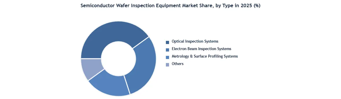
Based on Type: The market is segmented into Optical Inspection Systems, Electron Beam Inspection Systems and Others. The Optical Inspection Systems segment held the largest Semiconductor Wafer Inspection Equipment Market share in 2025. This is attributed to its widespread adoption and efficiency for detecting surface defects and pattern issues on semiconductor wafers. The Electron Beam Inspection Systems accounted the second largest share of the global market in 2025. This is because the system plays a major role in identifying minute defects, ensuring the integrity of advanced semiconductor devices.

Semiconductor Wafer Inspection Equipment Market

Semiconductor Wafer Inspection Equipment Market Regional Insights

Asia Pacific Semiconductor Wafer Inspection Equipment Market dominated the global market in 2025. China held the major share in the regional market. This is attributed to the significant presence of top semiconductor manufacturers, increasing investments by the government in the semiconductor industry and huge demand for consumer electronics. China, South Korea, Japan and Taiwan are the countries that highly benefit from strong semiconductor industries and substantial R&D investments. The need of precise wafer inspection has been rising due to the proliferation of IoT devices, 5G networks, and AI applications for optimal performance and high yield in semiconductor production.

North America Semiconductor Wafer Inspection Equipment Market held the second-largest share in 2025. This is attributed to the significant presence of established players such as KLA Corporation and the rising focus on advanced node technologies with high-performance computing applications. The United States is the key market for Semiconductor Wafer Inspection Equipment, driven by high investments from leading semiconductor manufacturers and strong R&D ecosystem. The need for wafer inspection solutions in the region is majorly being fuelled by the increasing demand for advanced consumer electronics, automotive electronics, and communication devices.

Semiconductor Wafer Inspection Equipment Market Scope: Inquire Before Buying

Semiconductor Wafer Inspection Equipment Market
Report Coverage Details
Base Year: 2025 Forecast Period: 2026-2032
Historical Data: 2020 to 2025 Market Size in 2025: 6.92 USD Billion
Forecast Period 2026-2032 CAGR: 8.22% Market Size in 2032: 12.03 USD Billion
Segments Covered: by Type Optical Inspection Systems
Electron Beam Inspection Systems
Metrology & Surface Profiling Systems
Others
by Inspection Type Patterned Wafer Inspection
Unpatterned Wafer Inspection
by Wafer Size 100 mm
150 mm
200 mm
300 mm
by Application Defect Inspection
Metrology
Wafer Edge Inspection
Surface Inspection
Others


Semiconductor Wafer Inspection Equipment Market, by Region

North America (United States, Canada and Mexico)
Europe (UK, France, Germany, Italy, Spain, Sweden, Austria and Rest of Europe)
Asia Pacific (China, South Korea, Japan, India, Australia, Indonesia, Malaysia, Vietnam, Taiwan, Bangladesh, Pakistan and Rest of APAC)
Middle East and Africa (South Africa, GCC, Egypt, Nigeria and Rest of ME&A)
South America (Brazil, Argentina Rest of South America)

Semiconductor Wafer Inspection Equipment Key Players

1. Applied Materials, Inc. (California, USA)
2. Leica Microsystems (Wetzlar, Germany)
3. Hitachi High-Tech Corporation (Tokyo, Japan)
4. KLA Corporation (California, USA)
5. Lam Research Corporation (California, USA)
6. Onto Innovation (Massachusetts, USA)
7. Tokyo Electron Limited (Tokyo, Japan)
8. Veeco Instruments Inc. (New York, USA)
9. Camtek Ltd. (Migdal HaEmek, Israel)
10. Nordson Corporation (Ohio, USA)
11. SCREEN Semiconductor Solutions Co., Ltd. (Kyoto, Japan)
12. ASML Holding N.V. (Veldhoven, Netherlands)
13. Nikon Metrology (Leuven, Belgium)
14. Toray Engineering (Tokyo, Japan)
15. Microtronic (Munich, Germany)
16. Ueno Seiki (Tokyo, Japan)

Others

Table of Contents

1. Semiconductor Wafer Inspection Equipment Market : Executive Summary 1.1. Study Assumption and Market Definition 1.2. Scope of the Study 1.3. Executive Summary 1.3.1 Market Size (2025) & Forecast (2026-2032), 1.3.2 Market Size (Value USD Mn.) (Volume in 000'Units) and Market Share (%) - By Segments, Regions and Country 2. Semiconductor Wafer Inspection Equipment Market : Competitive Landscapes 2.1. MMR Competition Matrix 2.2. Key Players Benchmarking 2.2.1 Company Name 2.2.2 Headquarter 2.2.3 Product Portfolio 2.2.4 Technology Integration 2.2.5 Production Capacity (000'Units) 2.2.6 Pricing Strategy 2.2.7 Sustainability Initiatives 2.2.8 Market Share (%) 2.2.9 Revenue (2025) 2.2.10 R&D Investment 2.2.11 Aftermarket & Service Offerings 2.2.12 Regulatory & Standards Compliance 2.2.13 Geographical Presence 2.3 Competitive Positioning Of Top Key Players 2.4. Market Structure 2.4.1 Market Leaders 2.4.2 Market Followers 2.4.3 Emerging Players 2.5. Mergers and Acquisitions Details 2.6. Market Share & Competitive Positioning 2.6.1 Global market share analysis of key players 2.6.2 Regional market share (Americas, Europe, APAC, Japan) 2.6.3 Competitive ranking and leaderboard of top players 2.7. Product & Technology Benchmarking 2.7.1 Product portfolio comparison of major players 2.7.2 Technology adoption: AI/ML, multi-beam, hybrid inspection systems 2.7.3 Inspection speed, resolution, and throughput benchmarking 2.7.4 Advanced packaging inspection capability (3D ICs, TSV, fan-out) 2.8. Supply Chain & Manufacturing Capabilities 2.8.1 Production footprint by region 2.8.2 Critical component sourcing: optics, sensors, stages, e-beam columns 2.8.3 Supply chain risk assessment and mitigation strategies 2.8.4 Manufacturing efficiency and lead times 2.8.5 Vendor partnerships for critical subsystems 3. Semiconductor Wafer Inspection Equipment Market: Dynamics 3.1. Semiconductor Wafer Inspection Equipment Market Trends 3.2. Semiconductor Wafer Inspection Equipment Market Dynamics 3.2.1 Drivers 3.2.2 Restraints 3.2.3 Opportunities 3.2.4 Challenges 3.3. PORTER’s Five Forces Analysis 3.4. PESTLE Analysis 4. Regulatory & Compliance Framework 4.1 Overview of global regulations for semiconductor inspection equipment 4.2 Safety standards for electron beam, X-ray, and high-voltage tools 4.3 Environmental compliance: energy efficiency, emissions, and waste management 4.4 Industry standards: SEMI, ISO, and cleanroom-related certifications 4.5 Regional regulatory requirements: US, EU, China, Japan, South Korea 4.6 Impact of regulatory changes on procurement, installation, and operation 5. Pricing, Cost Structure & Procurement Analysis (2025) 5.1 Historical price analysis by type (2020–2025) 5.2 Price range analysis: optical vs e-beam vs advanced tools 5.3 Total Cost of Ownership (TCO) for fab buyers 5.4 Operating costs: maintenance, software, calibration, consumables 5.5 Procurement best practices for large fabs vs mid-size fabs 5.6 Vendor contract structures and upgrade cycle analysis 6. Technology Landscape & Innovation Outlook 6.1 Detailed overview of optical inspection innovations (brightfield, darkfield, UV) 6.2 Electron beam inspection advancements: multi-beam, high-resolution review 6.3 X-ray, IR, and acoustic inspection adoption in package & subsurface analysis 6.4 AI/ML-driven defect identification & reduction in false positives 6.5 Hybrid inspection systems integrating multiple technologies for sub-3nm nodes 6.6 Technology roadmap & readiness for High-NA EUV and <2nm process nodes 7. Demand-Side Analysis 7.1 Wafer starts and device production forecast 7.2 Demand assessment by application and wafer size 7.3 Inspection tools demand from logic vs memory manufacturers 7.4 Impact of AI, HPC, automotive, and consumer electronics 7.5 Value chain pull from OSATs due to advanced packaging growth 7.6 End-user buying behavior and investment cycles 8. Supply Chain Analysis 8.1 Global supply chain structure for wafer inspection equipment 8.2 Critical component dependency assessment (optics, sensors, stages, imaging modules) 8.3 Supplier landscape mapping for key subsystems and materials 8.4 Vendor risk analysis: capacity constraints, quality issues, logistics risks 8.5 Manufacturing footprint and production capabilities of major OEMs 8.6 Supply chain resilience and mitigation strategies for OEMs and 8.6.1 semiconductor fabs 9. Sustainability & Energy Consumption Analysis 9.1 Energy consumption benchmarking of optical vs. e-beam inspection tools 9.2 Environmental footprint assessment: power, cooling, and cleanroom load 9.3 Adoption of energy-efficient subsystems and green design practices 9.4 OEM sustainability initiatives and carbon-reduction commitments 9.5 Waste management and end-of-life handling of inspection equipment 9.6 Impact of sustainability regulations on equipment selection and procurement 10. Installed Base & Replacement Cycle 10.1 Global installed base assessment by type (2025) 10.2 Age profile analysis of deployed inspection systems in fabs and foundries 10.3 Replacement cycle trends and upgrade intervals for optical and e-beam tools 10.4 Demand drivers for refurbishment, retrofits, and module upgrades 10.5 New tool vs. upgrade decision frameworks across IDMs, foundries, and OSATs 10.6 Installed base expansion forecast linked to capacity additions and node transitions 11. Customer Procurement & Decision Criteria 11.1 Key evaluation parameters: resolution, throughput, cost, uptime 11.2 Tool qualification and benchmarking process in fabs 11.3 Procurement cycles and approval gates for new systems 11.4 Impact of technology node transitions on purchase decisions 11.5 Vendor selection criteria: reliability, service, software support 11.6 Decision frameworks for new tool vs. upgrade/retrofit options 12. Throughput & Productivity Analysis 12.1 Benchmarking throughput for optical vs. e-beam inspection tools 12.2 Yield and defect detection efficiency across tool types 12.3 Trade-off analysis: sensitivity vs. throughput 12.4 Tool uptime, MTBF, and maintenance cycle considerations 12.5 Integration with fab workflow and production scheduling 12.6 Productivity improvement initiatives and automation impact 13. Service, Calibration & Aftermarket Opportunity 13.1 Installed-base service revenue potential by OEM and region 13.2 Calibration and preventive maintenance schedules 13.3 Predictive maintenance, remote diagnostics, and monitoring tools 13.4 Service contracts, upgrades, and software updates 13.5 Training and technical support for fab operators 13.6 Opportunities for aftermarket modules, retrofits, and consumables 14. Standards, Certifications & Compliance Requirements 14.1 SEMI equipment interface and inspection standards (E10, E84, GEM, EDA) 14.2 ISO and cleanroom standards applicable to inspection tools 14.3 Calibration certifications and traceability requirements 14.4 Compliance with environmental and energy efficiency regulations 14.5 Safety standards for electron beam and X-ray tools 14.6 Impact of standards on procurement and vendor selection 15. End-User Buying Behavior & Procurement Trends 15.1 Foundry vs IDM Purchasing Patterns 15.2 Technical Requirements in Fab Specifications 15.3 Vendor Qualification Processes 15.4 Impact of Fab Expansion Cycles on Demand 15.5 Preferences for Long-Term Service Contracts 16. Market Opportunities & Investment Hotspots 16.1 Asia’s Growing Fab Capacity (Taiwan, Korea, Japan, China, India) 16.2 U.S. CHIPS Act-Driven Investments 16.3 EU Semiconductor Strategy Opportunities 16.4 Emerging Markets for Advanced Packaging Inspection 16.5 High-Growth Segments: Multi-Beam E-Beam, EUV Inspection 17. Global Semiconductor Wafer Inspection Equipment Market: Market Size and Forecast By Segmentation (By Value in USD Million and Volume in 000'Units) (2025-2032) 17.1. Global Semiconductor Wafer Inspection Equipment Market Size 17.1.1 and Forecast, By Type (2025-2032) 17.1.2 Optical Inspection Systems 17.1.3 Electron Beam Inspection Systems 17.1.4 Metrology & Surface Profiling Systems 17.1.5 Others 17.2. Global Semiconductor Wafer Inspection Equipment Market Size and Forecast, By Inspection Type (2025-2032) 17.2.1 Patterned Wafer Inspection 17.2.2 Unpatterned Wafer Inspection 17.3. Global Semiconductor Wafer Inspection Equipment Market Size and Forecast, By Wafer Size (2025-2032) 100 mm 150 mm 200 mm 300 mm 17.4. Global Semiconductor Wafer Inspection Equipment Market Size and Forecast, By Application (2025-2032) 17.4.1 Defect Inspection 17.4.2 Metrology 17.4.3 Wafer Edge Inspection 17.4.4 Surface Inspection 17.4.5 Others 17.5 Global Semiconductor Wafer Inspection Equipment Market Size and Forecast, By End User Industry (2025-2032) 17.5.1 Semiconductor Manufacturers 17.5.2 Foundries 17.5.3 Integrated Device Manufacturers (IDMs) 17.5.4 OSAT (Outsourced Semiconductor Assembly and Test) 17.5.5 Others 17.6. Global Semiconductor Wafer Inspection Equipment Market Size and Forecast, By Region (2025-2032) 17.6.1 North America 17.6.2 United States 17.6.3 Canada 17.6.4 Mexico 17.6.5 Europe 17.6.6 United Kingdom 17.6.7 France 17.6.8 Germany 17.6.9 Italy 17.6.10 Spain 17.6.11 Sweden 17.6.12 Russia 17.6.13 Rest of Europe 17.6.14 Asia Pacific 17.6.15 China 17.6.16 South Korea 17.6.17 Japan 17.6.18 India 17.6.19 Australia 17.6.20 New Zealand 17.6.21 Indonesia 17.6.22 Philippines 17.6.23 Malaysia 17.6.24 Vietnam 17.6.25 Thailand 17.6.26 Taiwan 17.6.27 Rest of Asia Pacific 17.6.28 Middle East and Africa 17.6.29 South Africa 17.6.30 GCC 17.6.31 Turkey 17.6.32 Egypt 17.6.33 Nigeria 17.6.34 Rest of ME&A 17.6.35 South America 17.6.36 Brazil 17.6.37 Argentina 17.6.38 Colombia 17.6.39 Chile 17.6.40 Rest Of South America 18. Company Profile: Key Players 18.01. Zeiss 18.01.1 Company Overview 18.01.2 Business Portfolio 18.01.3 Financial Overview 18.01.4 SWOT Analysis 18.01.5 Strategic Analysis 18.02. KLA Corporation 18.03. Applied Materials 18.04. ASML Holding NV 18.05. Onto Innovation 18.06. Hitachi High-Tech 18.07. Lasertec Corporation 18.08. Nikon Metrology, LLC 18.09. JEOL 18.10. Camtek 18.11. SCREEN Semiconductor Solutions Co., Ltd. 18.12. Microtronic 18.13. Toray Engineering Co., Ltd. 18.14. Bruker Corporation 18.15. Nova Measuring Instruments Ltd. 18.16. UENO SEIKI CO., LTD. 18.17. confovis GmbH 18.17.1 Others 19. Key Findings 20. Future Outlook and Opportunity Landscape 21. Semiconductor Wafer Inspection Equipment Market: Research Methodology

Custom Market Research Services

We Will Customise The Research For You, In Case The Report Listed Above Does Not Meet With Your Requirements